- 您现在的位置:买卖IC网 > Sheet目录1991 > CS4339-KSZR (Cirrus Logic Inc)IC DAC STER 24BIT 96KHZ 8-SOIC
3
CS4334/5/8/9
LIST OF TABLES
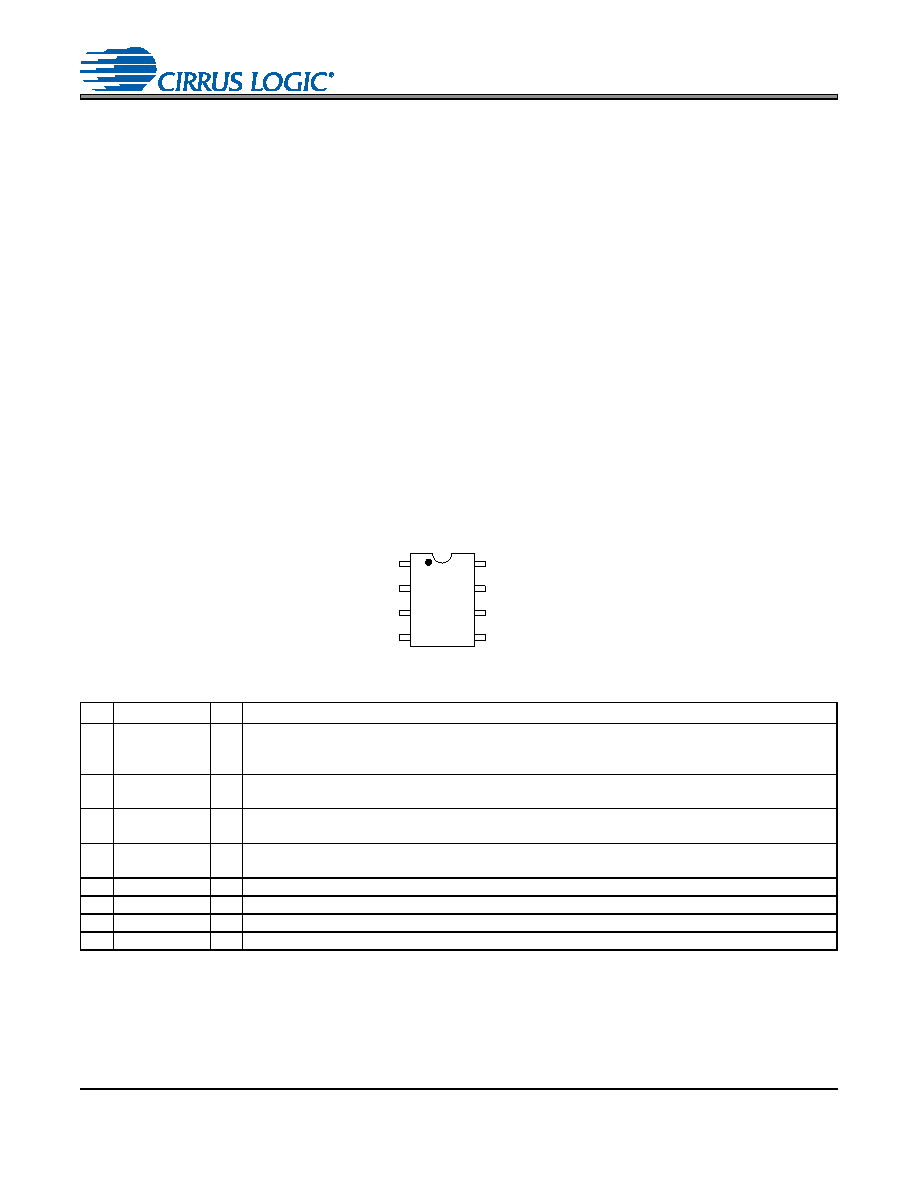
PIN DESCRIPTIONS
No.
Pin Name
I/O
Pin Function and Description
1SDATA
I
Serial Audio Data Input - Two’s complement MSB-first serial data is input on this pin. The data is
clocked into the CS4334/5/8/9 via internal or external SCLK, and the channel is determined by
LRCK.
2DEM/SCLK
I
De-Emphasis/External Serial Clock Input - Used for de-emphasis filter control or external serial
clock input.
3
LRCK
I
Left/Right Clock - Determines which channel is currently being input on the Audio Serial Data
Input pin, SDATA.
4MCLK
I
Master Clock - Frequency must be 256x, 384x, or 512x the input sample rate in BRM and either
128x or 192x the input sample rate in HRM.
5AOUTR
O
Analog Right Channel Output - Typically 3.5 Vp-p for a full-scale input signal.
6AGND
I
Analog Ground - Analog ground reference is 0V.
7VA
I
Analog Power - Analog power supply is nominally +5 V.
8AOUTL
O
Analog Left Channel Output - Typically 3.5 Vp-p for a full-scale input signal.
SERIAL DATA INPUT
SDATA
AOUTL
ANALOG LEFT CHANNEL OUTPUT
DE-EMPHASIS / SCLK
DEM/SCLK
VA
ANALOG POWER
LEFT / RIGHT CLOCK
LRCK
AGND
ANALOG GROUND
MASTER CLOCK
MCLK
AOUTR
ANALOG RIGHT CHANNEL OUTPUT
7
2
6
3
5
4
8
1
发布紧急采购,3分钟左右您将得到回复。
相关PDF资料
CS4340-CZZ
IC DAC 24BIT 96KHZ 101DB 16TSSOP
CS4341-CZZ
IC DAC STER 24BIT 96KHZ 16TSSOP
CS4341A-KSZ
IC DAC STER 24BIT 192KHZ 16SOIC
CS4351-DZZ
IC DAC STER 112DB 192KHZ 20TSSOP
CS4352-DZZ
IC DAC STER 102DB 192KHZ 20TSSOP
CS4354-CSZ
IC DAC 24BIT SRL 14SOIC
CS4360-KZZ
IC DAC STER 6CH 102DB 28TSSOP
CS4361-CZZR
IC DAC STER 6CH 105DB 20-TSSOP
相关代理商/技术参数
CS4-34
制造商:SUPERWORLD 制造商全称:Superworld Electronics 功能描述:POWER TRANSFORMER
CS4340
制造商:CIRRUS 制造商全称:Cirrus Logic 功能描述:24-Bit, 96 kHz Stereo DAC for Audio
CS4340_05
制造商:CIRRUS 制造商全称:Cirrus Logic 功能描述:24-Bit, 96 kHz Stereo DAC for Audio
CS4340A
制造商:CIRRUS 制造商全称:Cirrus Logic 功能描述:24-Bit, 192 kHz Stereo DAC for Audio
CS4340A_05
制造商:CIRRUS 制造商全称:Cirrus Logic 功能描述:24-Bit, 192 kHz Stereo DAC for Audio
CS4340A-KS
制造商:Rochester Electronics LLC 功能描述: 制造商:Cirrus Logic 功能描述:
CS4340A-KSR
制造商:Rochester Electronics LLC 功能描述: 制造商:Cirrus Logic 功能描述:
CS4340A-KSZ
功能描述:数模转换器- DAC IC 24-Bit 192kHz Stereo DAC for Audio RoHS:否 制造商:Texas Instruments 转换器数量:1 DAC 输出端数量:1 转换速率:2 MSPs 分辨率:16 bit 接口类型:QSPI, SPI, Serial (3-Wire, Microwire) 稳定时间:1 us 最大工作温度:+ 85 C 安装风格:SMD/SMT 封装 / 箱体:SOIC-14 封装:Tube